


|
Author: Dr Yu-Han Chang, Senior Technology Analyst at IDTechEx
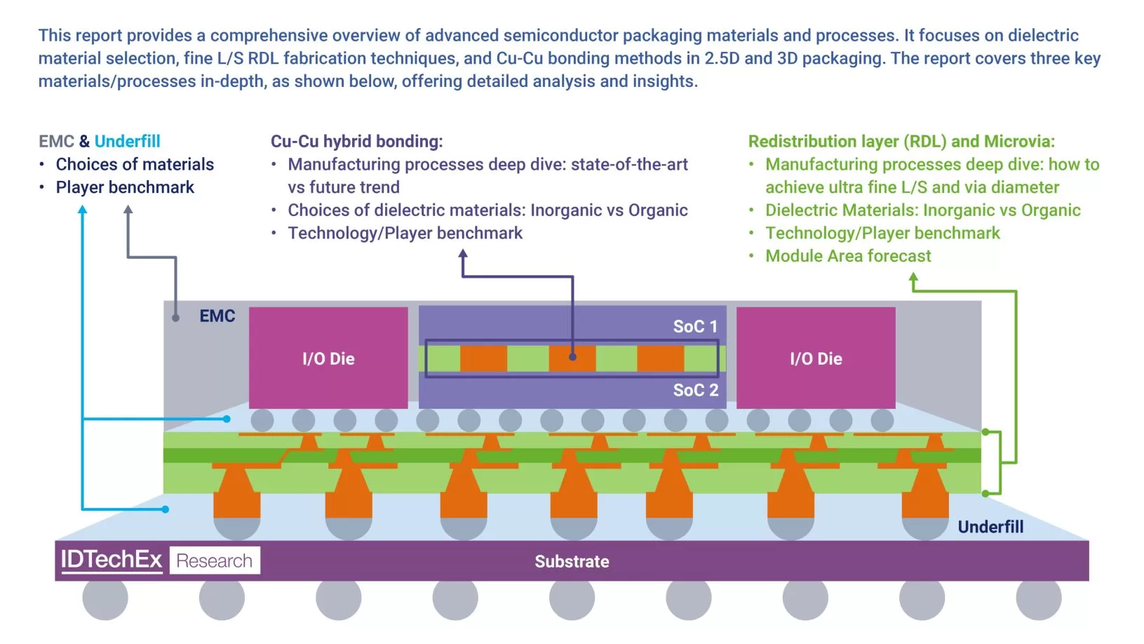
The semiconductor industry continually pushes packaging technology boundaries to meet the demand for higher chip performance and efficiency. Bandwidth is one of the critical factors defining the amount of data transmitted between dies on a package. Bandwidth, crucial for communication speed and efficiency, is impacted by factors such as IO/mm and Datarate/IO, which are, in turn, influenced by the dielectric materials selected for 2.5D and 3D packaging. This article explores the technology trends in dielectric materials for both 2.5D and 3D packaging, with insights drawn from IDTechEx's market report on the topic, “Materials and Processing for Advanced Semiconductor Packaging 2024-2034“. |
|
|
|
|
||
|
Scope of “Materials and Processing for Advanced Semiconductor Packaging 2024-2034”. Source: IDTechEx |
||
|
2.5D packaging:
For 2.5D packaging, achieving high bandwidth relies on the redistribution layer (RDL) within the package, where features like Line/Space (L/S), via, and pad dimensions are important. However, traditional inorganic dielectric materials like SiO2, though capable of achieving fine L/S, suffer from high dielectric constants (Dk=3.9) and are tied to the Si manufacturing technique. This hinders high-speed communication and presents costly challenges. Consequently, researchers are exploring organic alternatives with lower dielectric constants to enhance performance and reduce costs.
Organic dielectric materials emerge as promising alternatives for advanced semiconductor packaging, offering lower dielectric constants and cost advantages. However, selecting suitable organic dielectrics demands careful consideration of key parameters. IDTechEx's “Materials and Processing for Advanced Semiconductor Packaging 2024-2034” report identifies five critical parameters crucial for organic dielectrics, including Dk (dielectric constant) and Df (loss tangent), CTE (Coefficient of Thermal Expansion), Elongation, Young’s modulus, and Moisture absorption. Ideally, one would expect to have materials that exhibit low Dk and Df, compatible CTE with Si and Cu, high elongation value, and a moderate Young’s modulus to provide stability to the package. However, material selection entails trade-offs; for example, low Dk polymers may exhibit higher coefficients of thermal expansion (CTE), impacting device reliability and packaging architectures. Thus, achieving a balance among these parameters is critical for successful material selection in semiconductor packaging.
3D packaging:
Reducing the pitches between solder bumps has been a continuous advancement in the evolution of 3D packaging. However, such an approach presents challenges in establishing reliable electrical connections due to reduced bump height and surface area, necessitating precise manufacturing processes. Thermocompression Bonding (TCB) addresses this by enabling fine-pitch bonding as small as 10μm, although issues such as Intermetallic Compound (IMC) formation and solder ball bridging persist. To overcome these challenges, Cu-Cu Hybrid Bonding technology embeds metal contacts between dielectric materials and employs heat treatment for copper atom diffusion, eliminating soldering-related bridging problems and enhancing reliability in high-performance component packaging. It is considered a promising solution for the semiconductor industry, pushing the boundaries of miniaturization and performance in electronic devices.
Currently, hybrid bonding relies on inorganic dielectric materials like SiO2 or SiCN for insulation, which struggle with achieving fine-scale topography patterns and demand front-end manufacturing techniques. Alternatively, organic dielectrics, akin to the benefit it brings to 2.5D packaging, offer benefits such as low-k properties, reducing RC delay and insertion loss, resisting Cu migration, and tolerating defects and warpage better. However, using organic dielectrics for 3D hybrid bonding is still in the R&D phase due to challenges like elevated bonding temperatures (memory applications limit the bonding temperature to be below 250°C and in certain applications (such as displays) that contain sensitive materials embedded in the deck that cannot sustain high temperatures, the bonding temperature requirement must be reduced to 150°C. Furthermore, CMP compatibility with polymers remains a critical issue. Half-cured polymer's characteristics, including low modulus, viscoelastic behavior, and adhesion, pose challenges for ensuring Cu surface reliability during CMP. Modulus differences between Cu and polymer further complicate Cu protrusion formation.
IDTechEx's “Materials and Processing for Advanced Semiconductor Packaging 2024-2034” report suggests that if their properties are enhanced, organic dielectrics may become viable for hybrid bonding. If successful, integrating organic materials into mass production processes could prompt OSAT companies to adopt hybrid bonding more widely. This shift could broaden the technology's availability beyond a few foundries, as organic dielectrics offer the potential to ease stringent manufacturing and cleanroom standards associated with inorganic materials.
The report offers a structured overview of advanced semiconductor packaging in four main sections. The first part covers technology, trends, applications, and the ecosystem. The second part delves into 2.5D packaging processes, exploring dielectric materials, RDL fabrication, and material selection. Detailed analyses, player evaluations, and future trends are provided. Moving beyond 2.5D, the third part focuses on Cu-Cu hybrid bonding for 3D die stacking, offering insights into manufacturing processes, material selection, and case studies. Finally, the report includes a 10-year market forecast for Organic Dielectric Advanced Semiconductor Packaging, providing industry perspectives on market growth and trends.
To find out more about this report, including downloadable sample pages, please visit www.IDTechEx.com/MatsforASP.
For the full portfolio of semiconductor market research from IDTechEx, please see www.IDTechEx.com/Research/Semiconductors |